- Cart
- |
- Personal Center
- |
info@idealphotonics.com


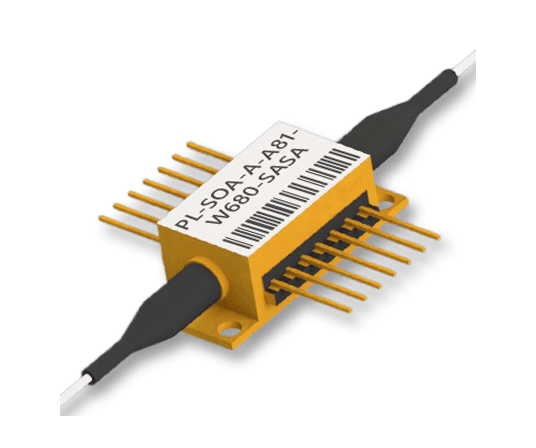


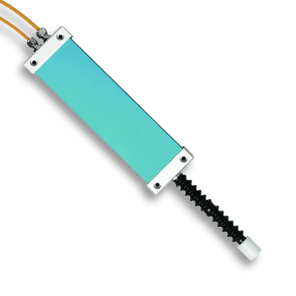
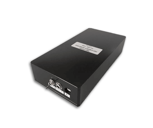


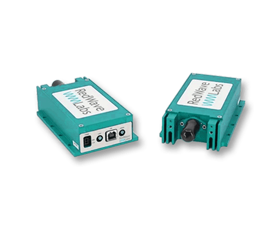


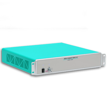

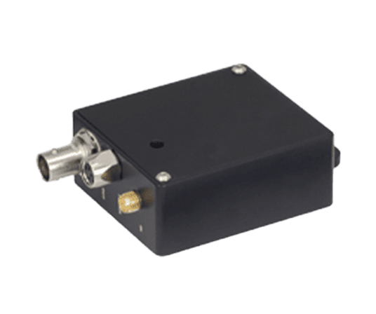
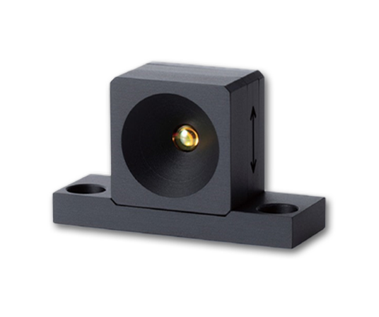
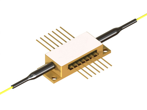
1080nm High-Gain Semiconductor Optical Amplifier
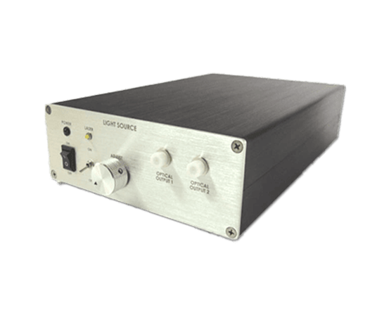
A high gain semiconductor optical amplifier designed for the 1080nm wavelength band. By using proprietary anti reflective coating technology and ridge waveguide design, high fidelity and high gain amplification of weak optical signals can be achieved. This series of products features high gain, high saturation output power, and high polarization extinction ratio, and offers two different product forms: component level butterfly package SOA (suitable for system integration) and modular integrated amplifier (controller all-in-one, plug and play) to meet the diverse needs of scientific research experiments and commercial systems.
Product features:High gain coefficient; narrowband optimized amplification; low-power operation; excellent signal-to-noise ratio; superior temperature stability
Part Number:MP-SOA-1080-35db-25-XA
Application area:Precision laser measurement | quantum optics experiment | fiber optic sensing system | medical diagnostic equipment | research-grade optical system
Add to Cart Request for Quotation Consult Favorite
Operating Wavelength Operating Bandwidth
1080nm 25nm
Detailed Specifications
Recommended Operating Conditions
@ CW, housing mounted on a heat sink at room temperature
Parameter | Min. | Typ. | Max. | Unit |
Chip Temperature | 20 | 25 | 30 | °C |
Forward Current | — | 400 | 500 | mA |
Input Optical Power | -40 | -25 | 10 | dBm |
* The current for maximum gain spectral width may vary by batch.
Gain Characteristics
@ CW, 25°C,400 mA, input signal: -25 dBm at maximum gain wavelength
Parameter | Min. | Typ. | Max. | Unit |
Small-Signal Gain @ 400 mA | 31 | 35 | — | dB |
Saturated Output Power @ 400 mA (-3 dB) | 12 | 15 | — | dBm |
Average Gain Wavelength | 1070 | 1080 | 1095 | nm |
Gain Bandwidth (FWHM) | 20 | 25 | — | nm |
Noise Figure | — | 7 | — | dB |
Noise Figure Formula:
NF=10log 10(2P ase /Ghν)
[D. Baney et al., Fiber Technology, 6, 122 (2000)]
Amplified Spontaneous Emission (ASE) Characteristics
@ CW, 25°C, 400 mA, no input signal
Parameter | Min. | Typ. | Max. | Unit |
Output Power (Per Port) | — | 40 | — | mW |
Forward Voltage | — | 1.5 | 1.8 | V |
Average Wavelength | 1070 | 1080 | 1095 | nm |
Bandwidth (FWHM) | 20 | 25 | — | nm |
Ripple (RMS)** | — | 0.04 | 0.2 | dB |
Polarization Extinction Ratio (PER) | 15 | 18 | — | dB |
Polarization | — | TE | — | — |
** Measured within 1 nm range near the spectral peak with 20 pm resolution.
Absolute Maximum Ratings
Parameter | Min. | Max. | Unit |
Output Optical Power | — | 500 | mW |
Input Optical Power | — | 20 | dBm |
Forward Current | — | 800 | mA |
Reverse Voltage | — | 2 | V |
TEC Current | — | 3 | A |
TEC Voltage | — | 4 | V |
Chip Operating Temperature | 10 | 40 | °C |
Housing Operating Temperature | 0 | 70 | °C |
Storage Temperature | -40 | 85 | °C |
Lead Soldering Temperature (Max. 10 s, max housing temperature 120 °C) | — | 300 | °C |
Fiber Bend Radius | 3 | — | cm |
Typical performance (for reference only)
@CW, the case is mounted on room temperature heatsink
Gain spectra at different currents

Gain and Output power vs. Input signal

Gain spectra at different input signals

Spectra of amplified optical signal

ASE spectra(no input signal)

Output power at different input signals

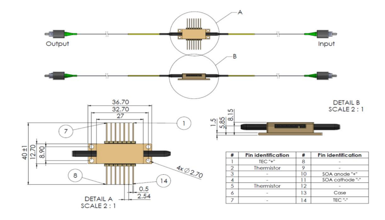
Thermistor Specifications | Fiber Specifications | |||||
Parameter | Value | Unit | Parameter | PM980 | HI1060 | Unit |
Type | NTC | — | Numerical Aperture, typical | 0.12 | 0.14 | — |
Resistance @ 25 °C | 10 ± 0.1 | kΩ | Cutoff Wavelength | 900 ± 70 | 920 ±50 | Nm |
Beta (25–85 °C) | 3435 ± 1% | K | Mode Field Diameter (@ 1060 nm) | 6.6 ± 0.3 | 6.2 ± 0.3 | μm |
| Cladding Diameter | 125±1 | 125±1 | μm | ||
Coating Diameter | 245±15 | 245±15 | μm | |||
Loose Tube Diameter (Optional) | 900 | 900 | μm | |||
Connector | FC/APC (narrow key) | |||||
Connector Alignment aligned with PANDA fiber | ||||||
Output light is polarized along the slow axis of the PM fiber. | ||||||
Operating InstructionsSafety and Operating Instructions
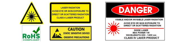
The light emitted by this device is invisible and harmful to human eyes. Do not look directly at the fiber connector during operation. Appropriate laser safety goggles must be worn when operating with the connector uncovered.
Absolute maximum ratings may only be applied to the device for a short time. Long-term operation at or simultaneous exposure to multiple maximum ratings may cause device damage and reduce reliability. Operation beyond the maximum ratings may lead to device failure and safety risks. A matched power supply shall be used to ensure that the maximum forward current is not exceeded.
Devices mounted on heat spreaders require a proper heat sink. Secure the device to the heat sink with four screws (cross-tightened with an initial torque of 0.075 N·m and a final torque of 0.15 N·m) or clamps. The flatness deviation of the heat sink surface shall be less than 0.05 mm. Indium foil or flexible thermal interface materials are recommended between the device base and the heat sink. Thermal grease is not recommended.
Avoid optical back-reflection, which may degrade spectral performance and power stability, and cause catastrophic facet damage. The use of an optical isolator is strongly recommended to suppress back-reflection.
Do not pull the optical fiber. Do not bend the fiber with a bending radius less than 3 cm. Protect the fiber end-face from contamination and damage during installation. After removing the dust cap, clean the fiber end-face in one direction with lens wipes or cotton swabs moistened with isopropyl alcohol or ethanol. Only operate the device with clean fiber connectors.
ESD Protection – Electrostatic discharge is a major cause of unexpected product failure. Strict ESD protection measures must be taken. Maintain ESD control during installation, including anti-static wristbands, grounded work surfaces and standardized anti-static operation procedures.
--
Request for Quotation
We will reply to all your information about the product in time.
⇪