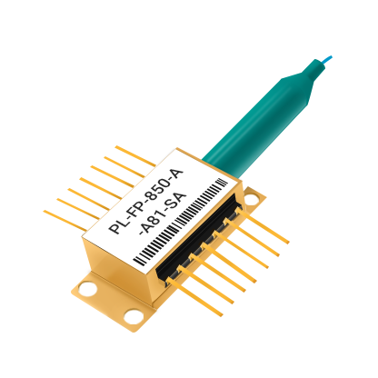
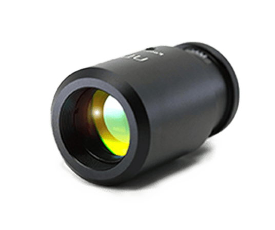
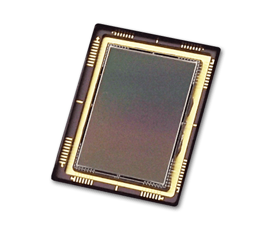
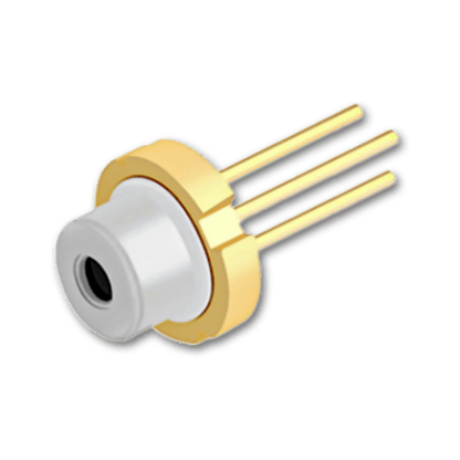
info@idealphotonics.com

Pulse Type Laser Diode

  • PCSEL laser diode

    IdealPhotonics' PCSEL diode, a vertical-cavity surface-emitting laser based on two-dimensional photonic crystal bandgap engineering, achieves high power (watt-level), narrow divergence angle (<1°), and single-mode lasing characteristics through precise control of photonic density of states via periodic nanostructures (lattice constant ≈ wavelength). Its innovative "asymmetric photonic crystal" design simultaneously breaks through beam quality (M² <1.05) in the visible to near-infrared band (400-1100nm).Utilizing two-dimensional photonic crystal bandgap technology (lattice accuracy ±1nm), it achieves a revolutionary combination of watt-level single-mode output and an ultra-narrow divergence angle of <0.5°. Its innovative "topology-optimized photonic crystal" structure simultaneously breaks through beam quality (M² <1.05) and 50GHz modulation bandwidth in the 400-1100nm band, enabling applications in AR holographic displays (10μm pixel accuracy), 4D... In three disruptive applications—LiDAR (0.01° angular resolution), terahertz communication (100Gbps)—power conversion efficiency has been increased to 60%, redefining the performance limits of surface-emitting lasers.

  • PLD laser diode

    IdealPhotonics' PLD diode is based on a thin-film fabrication technology using high-energy pulsed lasers (typically KrF/ArF excimer lasers or Nd:YAG lasers) to bombard targets. It achieves atomic-level material exfoliation and deposition in a vacuum/reactive gas environment using nanosecond-level pulses (energy density 1-10 J/cm²). Its innovative "dual-beam synchronous control" system can fabricate various functional thin films, including superconducting (e.g., YBCO), ferroelectric (e.g., PZT), and two-dimensional materials (e.g., graphene). These films exhibit high compositional fidelity (>99%) and film thickness control precision down to a single atomic layer (±0.01 nm), making them a core fabrication tool in cutting-edge fields such as quantum devices and flexible electronics.Employing high-energy pulsed lasers (such as 248nm KrF or 193nm ArF) and multi-target synergistic sputtering technology, atomic-level precision (±0.005nm) thin film deposition is achieved in an ultra-high vacuum environment of 10⁻⁶ Pa. Its innovative "real-time plasma spectral monitoring" system enables the control of compositional deviations in multi-component oxides (such as YBCO superconducting films).

  • 10+ 10 Years of Experience
  • 50 50 + Countries Bussiness
  • 10000 10k + Diodes sold worldwide
  • 30 30+ Invention patent
  • 10 10+ Advanced Optical Solutions