- Cart
- |
- Personal Center
- |
info@idealphotonics.com


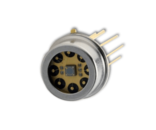


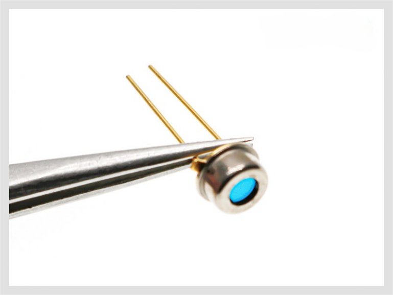
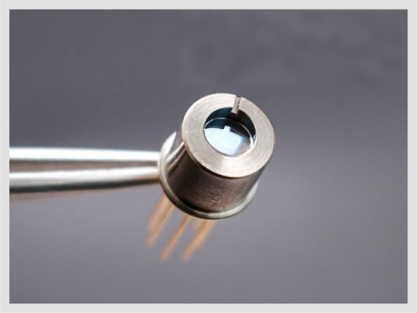
795nm 0.13mW GaAs SM Low-Power VCSEL Die(Group 2)
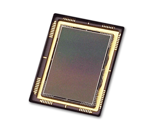
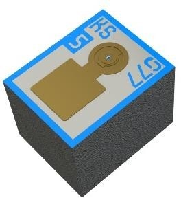
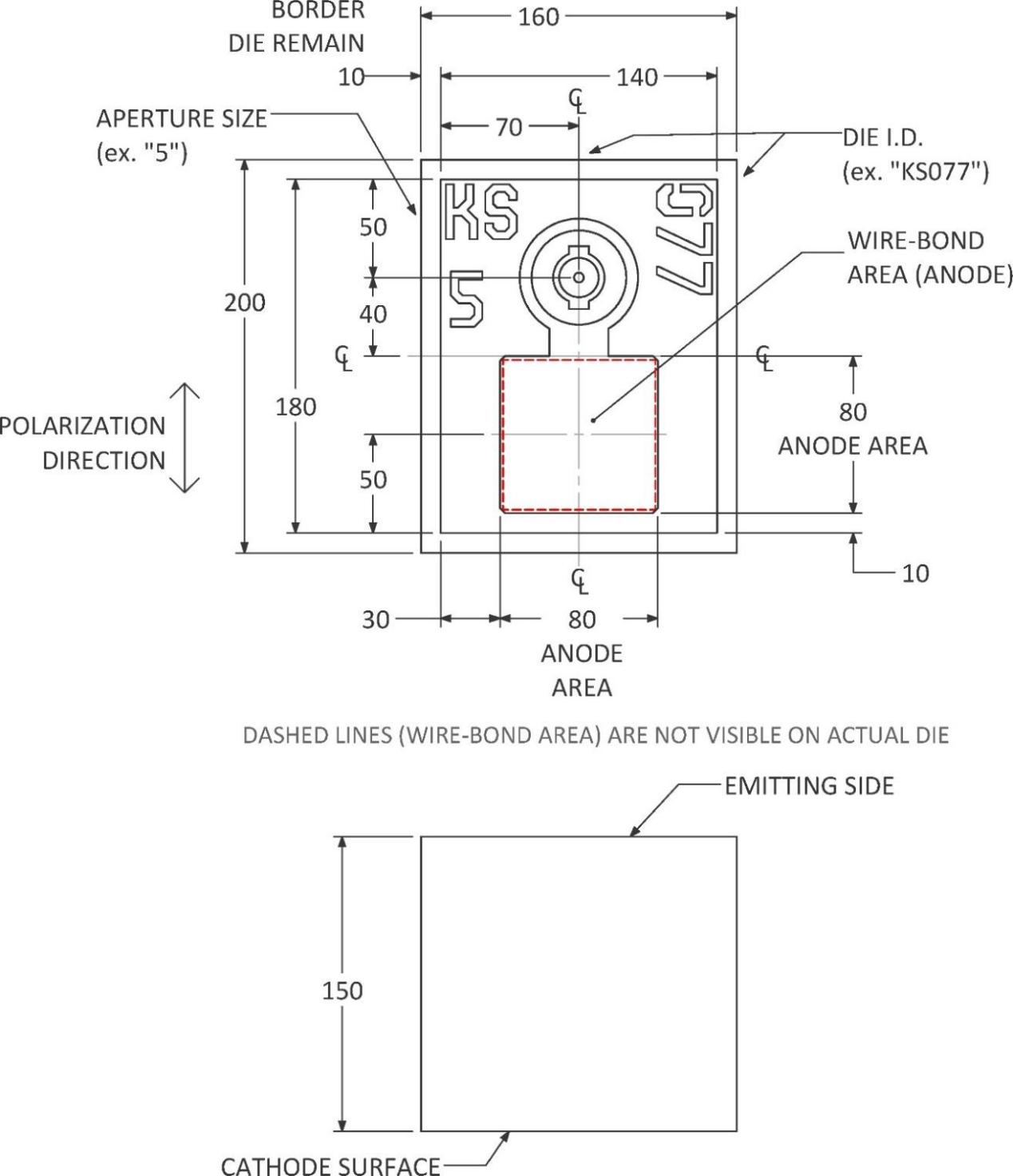
A Vertical-Cavity Surface-Emitting Laser (VCSEL) is a type of semiconductor laser whose laser beam emits perpendicularly from the top surface.Developed based on Gallium Arsenide (GaAs) semiconductor material, it is distinct from LEDs (Light-Emitting Diodes) and LDs (Laser Diodes). Its structure consists of mirror layers, an active region, and metal contact layers. The two emission mirrors are P-type and N-type Distributed Bragg Reflectors (DBR). The active region is composed of quantum wells. An ohmic contact is formed by depositing a metal contact layer on the surface of the P-type DBR, with a circular emission aperture fabricated on the P-type DBR for laser output.Die parameters: 2222; 795 nm; Single-mode; 1 M; S5, S6, S7; 0.13 mW; chip size 0.16×0.20 mm
Product features:Ultra-low power consumption;High-temperature stability;Single-mode lasing property;High-density integration capability;Fast response speed
Part Number:MP-VCS-795-0.13-DIE2-SM
Application area:High-temperature electronic devices | Optical Interconnection | Biosensing | Consumer Electronics | Aerospace Applications
Add to Cart Request for Quotation Consult Favorite
Center Wavelength
795nm
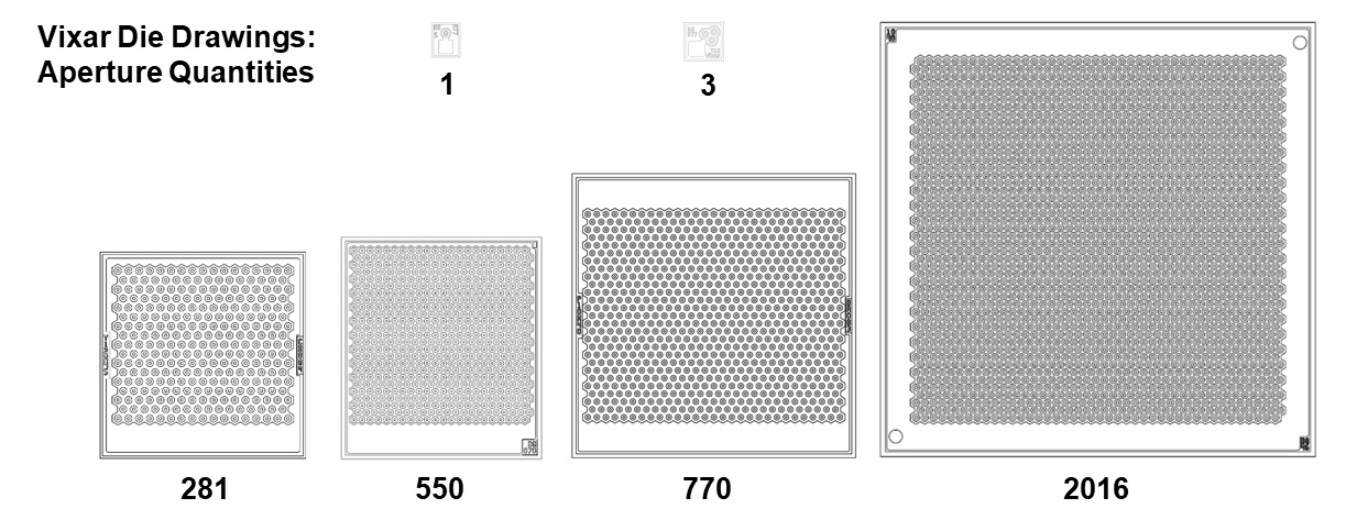
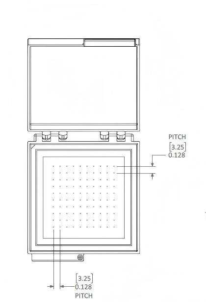
Vixar Mold Drawing: Number of Hole Diameters
We currently have the following standard parts available for sample and mass production
Standard portfolio – low-power chips
Wavelength | Mold details | Suggest Max. Peak power | Note |
Single-mode | |||
795nm | 0.16 mm x 0.20 mm single bore | 0.15mW | Line width < 100MHz, +/- 0.5nm polarization stabilized |
895nm | 0.16 mm x 0.20 mm single bore | 0.2mW | Line width < 100MHz, +/- 0.5nm polarization stabilized |
Multimodal | |||
680nm | 0.22 mm x 0.22 mm single bore | 7mW | Visible light, increased efficiency, non-Gaussian beam shape polarization stability |
Standard portfolio – High power chip – 850 nm
Mold details | Suggest Max. Peak power | Suggest Max. Peak power | Suggest Max. Peak power |
0.52 mm x 0.52 mm | 0.5W | 1W | 5W |
0.87 mm x 0.87 mm | 2W | 6W | 13W |
0.90 mm x 1.00 mm | 3W | 9W | 35W |
1.26 mm x 1.26 mm | 4W | 12W | 36W |
1.99 mm x 1.99 mm | 6W | 20W | 78W |
Standard portfolio – High power chip – 940 nm
Mold details | Suggest Max. Peak power | Suggest Max. Peak power | Suggest Max. Peak power |
0.87 mm x 0.87 mm | 2W | 6W | 13W |
0.90 mm x 1.00 mm | 3W | 8W | 35W |
0.90 mm x 1.00 mm | 4W | 12W | 110W |
1.26 mm x 1.26 mm | 4W | 11W | 36W |
1.99 mm x 1.99 mm | 6W | 20W | 76W |
VCSEL low-power chip GaAs 795nm Max. rating
Ta = 80°C
Parameters | symbol | value | |
Operating/soldering temperature DC = 100% | TS | Min. value Max. value | -20°C 110°C |
Storage temperature | Tstg | Min. value Max. value | -40°C 125°C |
Forward current (maintain single mode) DC operation; DC = 100%; TS = 75°C | If | Max. value | 1.5 mA |
Forward current DC operation; DC = 100%; TS= 75°C | If | Max. value | 3mA |
Reverse voltage | Not suitable for reverse operation | ||
ESD withstand voltage acc. to ANSI/ESDA/JEDEC JS-001 (HBM, Class 1A) | VESD | Max. value | 250 V |
Note: Beyond jue to Max. Stress in the rated range can cause permanent damage to the equipment.
Characteristics:
Ta = 80°C, IF = 1.4 mA; DC = 100% - Group 3
Parameters | symbol | value | |
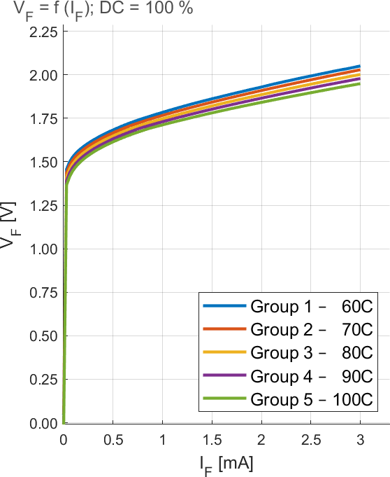
Forward current | VF | Typical values | 1.8 V |
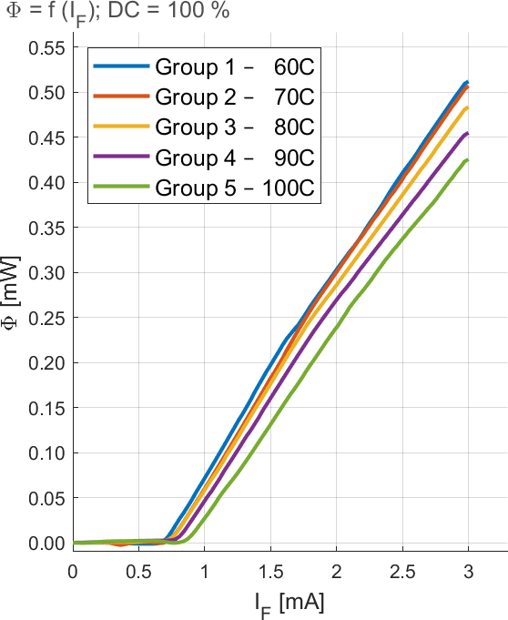
Output power | Φ | Typical values | 0.13 mW |
Threshold current | Ith | Typical values | 0.75 mA |
Slope performance | SE | Typical values | 0.21 W / A |
Single-mode suppression ratio | SMSR | Min. value | 20 dB |
Polarization extinction ratio5) | PER | Min. value | 15 dB |
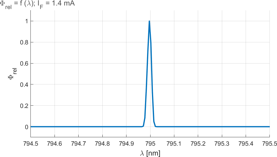
Peak wavelength | λpeak-v | Min. value Typical values Max. value | 794.5 nm 795 nm 795.5 nm |
Spectral line width | Λlinewidth | Max. value | 100 MHz |
FM modulation bandwidth | Fm | Min. value | 3.4 GHz |
Wavelength temperature coefficient | TCλ | Typical values | 0.055 nm / K |
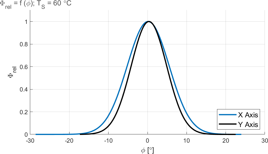
Half-peak full-width field of view (50% of Φmax) | φx φY | Typical values Typical values | 12° 12° |
1/e2 field of view | φx φY | Typical values Typical values | 20° 20° |
Note: Wavelength, output power varies depending on the operating temperature and voltage.
Relative Spectral Emission 1)
Emission characteristics 1)
Forward current 1) 2)
Optical Output Power 1) 2)
Packaging
Notes:
Depending on the mode of operation, these devices emit highly concentrated visible and non-visible light, which can be harmful to the human eye. Products containing these devices must follow the safety precautions given in IEC 60825-1.
Among other substances, the subassemblies of the device contain metal-filled materials, including silver. Metal-filled materials can be subject to environmental influences that contain aggressive substances. Therefore, we recommend that customers minimize the exposure of equipment to corrosive substances during storage, production and use. When tested using the above tests, devices that showed visible discoloration did not show performance deviations within the fault limits for the specified test duration.
The corresponding fault limits are described in the IEC60810.
terminology
1) Typical values: Due to the special conditions of the semiconductor device manufacturing process, typical data or computational associations of technical parameters can only reflect statistics. These do not necessarily correspond to the actual parameters of each product, which may differ from the typical values and calculation of the relevant or typical characteristic lines. These typical values data will be changed without notice due to technical improvements.
2) Test temperature: TA = 85°C ± 2°C
3) Dimensional tolerance: Unless otherwise specified in the drawing, the tolerance is specified in ±0.1 and the size is specified in mm.
4) Wavelength: Continuous wavelength measurement with a resolution ± 0.1 nm.
5) Polarization: Under mold stress conditions caused by mounting or encapsulation, the polarization extinction ratio decreases.
Ordering information
Description | Working mode | Order code |
Group 1 - Die; 2222; 795; S; 1M; S5,S6,S7; 0.13mW; 0.16X0.20mm | Ta = 60±10°C; IF = 1.4 mA; DC = 100%, 795nm | V00145 Group: 1 |
Group 2 - Die; 2222; 795; S; 1M; S5,S6,S7; 0.13mW; 0.16X0.20 | Ta = 70±10°C; IF= 1.4 mA; DC = 100%, 795nm | V00145 Group: 2 |
Group 3 - Die; 2222; 795; S; 1M; S5,S6,S7; 0.13mW; 0.16X0.20mm | Ta = 80±10°C; IF = 1.4 mA; DC = 100%, 795nm | V00145 Group: 3 |
Group 4 - Die; 2222; 795; S; 1M; S5,S6,S7; 0.13mW; 0.16X0.20mm | Ta = 90±10°C; IF = 1.4 mA; DC = 100%, 795nm | V00145 Group: 4 |
Group 5 - Die; 2222; 795; S; 1M; S5,S6,S7; 0.13mW; 0.16X0.20mm | Ta = 100±10°C; IF = 1.4 mA; DC = 100%, 795nm | V00145 Group: 5 |
--
Request for Quotation
We will reply to all your information about the product in time.
⇪