- Cart
- |
- Personal Center
- |
info@idealphotonics.com

















Superconducting-Silicon Photonic Integrated Quantum Photonic Chips Applied to Construct Quantum Entanglement Distribution Networks
2026-07-24 10:37:32177
Recently, a research team led by Li Hao, Shu Zhiyun, You Lixing from the Shanghai Institute of Microsystem and Information Technology, Chinese Academy of Sciences has made breakthroughs in superconducting-silicon photonic integrated quantum photonic chips and realized the construction of a scalable quantum entanglement distribution network connecting cryogenic nodes. The relevant research results were published in the Q1 journal npj Quantum Information under the title Multiuser entanglement distribution network across cryogenic nodes enabled by integrated photonic chips (DOI: https://doi.org/10.1038/s41534-026-01262-7).
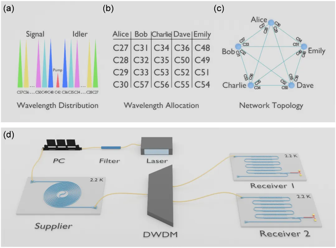
Figure 1: Schematic diagram of the architecture and experimental setup of the quantum entanglement distribution network between cryogenic chips
With the rapid advancement of quantum information science, scalable quantum networks, capable of distributing entanglement resources to multiple user nodes, will serve as the core infrastructure for applications including distributed quantum computing, quantum secure communication and quantum precision metrology. In practical scenarios, various types of quantum nodes such as quantum dots, ion traps and quantum memories operate under ultra-low temperature conditions. To realize the practical deployment of quantum networks, interconnection between cryogenic nodes becomes critically important, posing major challenges to network construction.
To address this cutting-edge challenge, based on their prior development of monolithic heterogeneously integrated entanglement receiver chips integrating pump filtering and single-photon detection functions, the team further demonstrated a scalable multi-user entanglement distribution network spanning multiple cryogenic quantum nodes using integrated photonic chips (see Figure 1). In this scheme, relying on spontaneous four-wave mixing (SFWM), a photonic chip embedded with a 1 cm-long silicon spiral waveguide acts as the entanglement transmitter chip. Operated at an ultra-low temperature of 2.2 K, it generates broadband energy-time entangled photon pairs and delivers them to other cryogenic nodes. Afterwards, the entangled photon pairs are multiplexed via standard dense wavelength division multiplexers (DWDM) and distributed to multiple cryogenically-cooled entanglement receiver chips.
Each entanglement receiver chip monolithically heterogeneously integrates silicon-based passive pump filters and superconducting nanowire single-photon detectors (SNSPDs). It can suppress milliwatt-level intense pump light prior to photon detection to avoid interference with entangled photon pair reception. Experimental characterization at 2.2 K shows the on-chip pump filter achieves an extinction ratio exceeding 56 dB, while the system detection efficiencies of two sets of on-chip SNSPDs reach 7.1% and 6.5% respectively (see Figure 2).
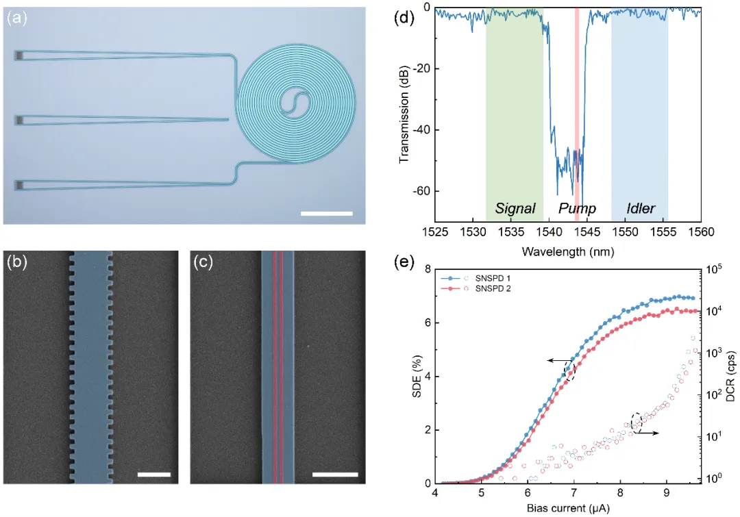
Figure 2: Fabrication results and performance characterization of cryogenic chips
To verify the feasibility of the proposed scheme, the research team constructed a fully connected quantum network with five user nodes utilizing ten entangled-photon wavelength channels. Under this network topology, each user node receives entangled photons from four distinct wavelength channels, enabling entanglement channel establishment between any pair of users. Measured under two sets of non-orthogonal measurement bases, the raw Franson two-photon interference visibilities of all ten channel combinations exceed 86% (see Figure 3), which significantly violates Bell’s inequality. This verifies the successful construction of the cryogenic-node quantum network architecture and demonstrates its promising application potential for future practical, scalable quantum networks.
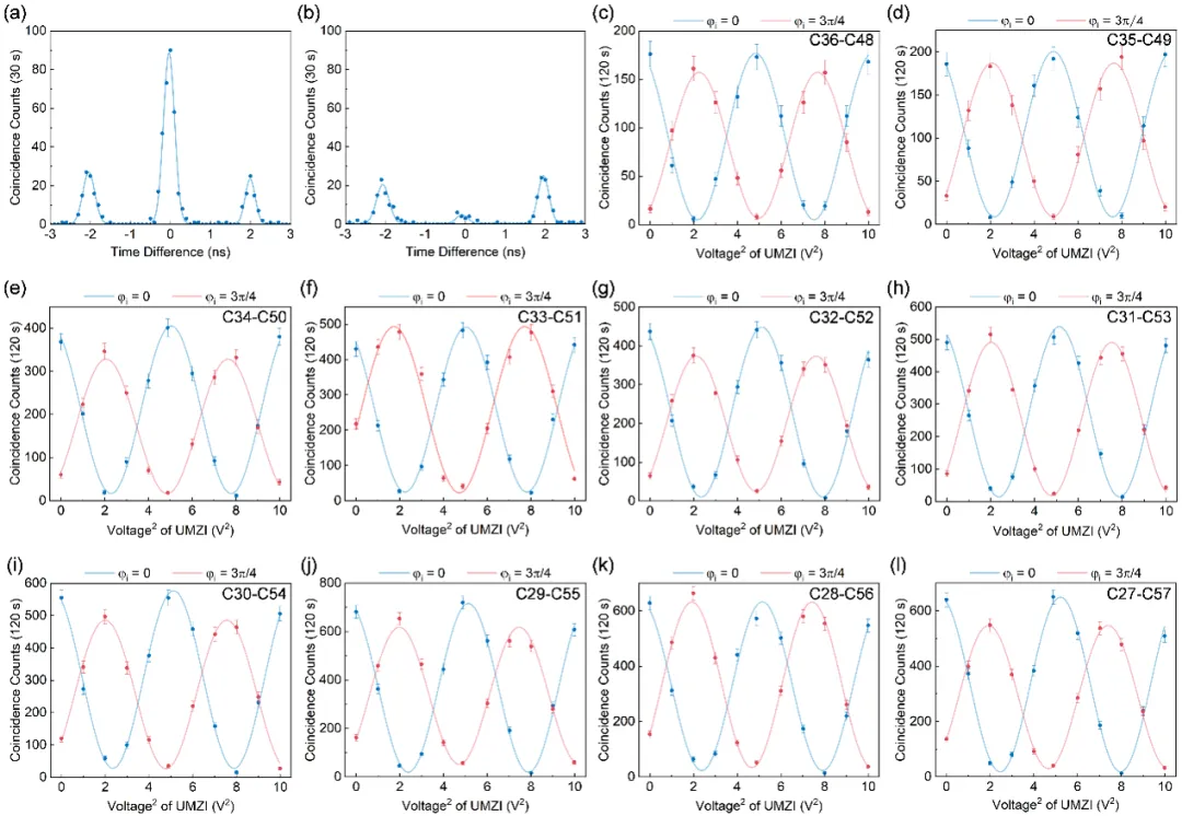
Figure 3: Two-photon interference characterization results of all ten channel combinations
Shu Zhiyun, a postdoctoral researcher at the Shanghai Institute of Microsystem and Information Technology, is the first author of the paper, and Researcher Li Hao serves as the corresponding author. This work was supported by the Major Project of Science and Technology Innovation 2030 (Grant No. 2023ZD0300100), Shanghai Major Quantum Special Project (Grant No. 2019SHZDZX01), and the National Natural Science Foundation of China (Grant Nos. U24A20320, 62401554).
Reference: Shanghai Institute of Microsystem and Information Technology, Chinese Academy of Sciences
Disclaimer:
The information content is sourced from the Internet. It does not represent the endorsement of viewpoints by this website and new media platforms, nor do we take responsibility for its authenticity. If you have objections regarding the copyright of texts, images or other materials, please contact us, and we will arrange relevant deletion accordingly. Industry news is for reference only, and no competing economic interests are involved.
Recommend
 10+
10 Years of Experience
10+
10 Years of Experience
 50
50 + Countries Bussiness
50
50 + Countries Bussiness
 10000
10k + Diodes sold worldwide
10000
10k + Diodes sold worldwide
 30
30+ Invention patent
30
30+ Invention patent
 10
10+ Advanced Optical Solutions
10
10+ Advanced Optical Solutions
⇪