- Cart
- |
- Personal Center
- |
info@idealphotonics.com
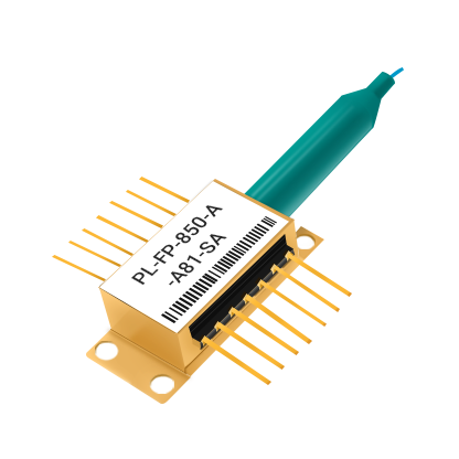


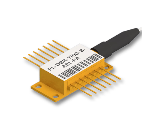


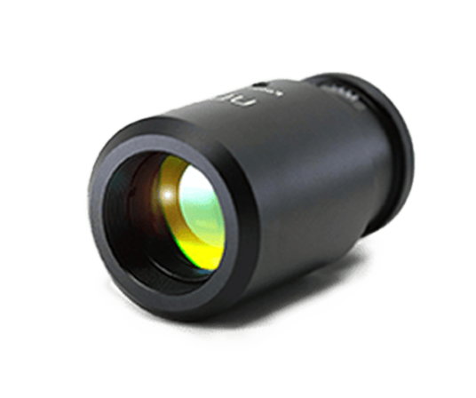


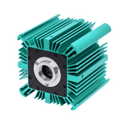
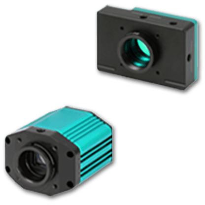


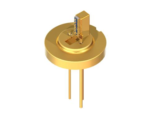
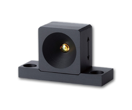
1150nm 230mW TypeA Gain Chip (TO Package)
A type A (straight stripe) gain chip with TO packaging, with a center wavelength of 1150nm, designed specifically for external cavity semiconductor lasers. The chip is coated with high reflectivity (HR) and anti reflectivity (AR) coatings on both end faces, and must rely on external frequency selective elements (such as diffraction gratings) to generate laser light, thereby achieving a wide tuning range and high edge mode suppression ratio.
Product features:TO package;Wide gain bandwidth;Low noise;High output power;Easy integration
Part Number:MP-GC-1150-90-230-To-A
Application area:Optical fiber communication | LiDAR | Medical equipment | Sensor networks | Industrial processing
Add to Cart Request for Quotation Consult Favorite
Center wavelength Tuning range Output power Forward current
1150nm 90nm 230mW 600mA
Recommended operating conditions
Parameters | Min. value | Typical values | Max. value | unit |
Radiator temperature | 20 | 25 | 30 | ℃ |
Forward current* | 600 | mA | ||
Optical feedback** | 20 | % |
*Max. No self-excited laser is generated when the current is reached
** Coupling efficiency with chip is not included
Tunable characteristics
Batch Qualified @ CW, 25C, 600mA, Outer Cavity with Littman Configuration with 20% Feedback
Parameters | Min. value | Typical values | Max. value | unit |
Max. Power wavelength | 1145 | 1160 | 1175 | nm |
The output power @780nm | 150 | 230 | mW | |
Tuning range center wavelength | 1135 | 1150 | 1165 | nm |
Tuning range width (full) | 90 | nm | ||
The side-mode suppression ratio (SMSR) is @780nm | 60 | dB |
Amplified spontaneous radiation (ASE) characteristics
Test each sample @ CW, 25C, 600mA, no feedback
Parameters | Min. value | Typical values | Max. value | unit |
Output power | 1.5 | mW | ||
Forward voltage | 1.5 | 2.2 | V | |
Average wavelength | 1145 | nm | ||
Bandwidth (FWHM)* | 70 | nm | ||
Fast axis beam divergence (FWHM). | 35 | 42 | 45 | deg |
Slow axis beam divergence (FWHM). | 3 | 5 | 11 | deg |
polarization | TE |
*Radiation is coupled in a lensless single-mode fiber and measured at 1 nm resolution by OSA.
Chip parameters
Parameters | Min. value | Typical values | Max. value | unit |
Chip length | 3 | mm | ||
Backward reflection on the front | 0.1 | % | ||
Back reflection on the back | 90 | 99 | % |
For Max. rated parameters
Parameters | Min. value | Max. value | unit |
Forward current @ 20% feedback | 800 | mA | |
Optical feedback (excluding coupling with chip) | 30 | % | |
Reverse voltage | 1 | V | |
Operating temperature (above dew point) | -10 | 60 | ℃ |
Storage temperature (in its original sealed packaging) | -40 | 85 | ℃ |
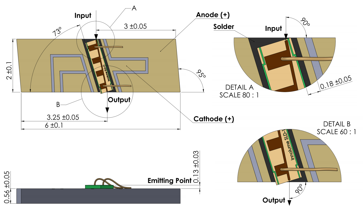
Drawings

General parameters
There are two types of outer cavity lasers that use diffraction gratings: Littrow and Littman/Metcalf. The primary diffraction light of the Littrow type diffraction grating is fed directly into the semiconductor laser and oscillated by resonating with the low-reflection film (LR) of the vertical end face. Since diffraction is performed only once, a larger optical output than the Littman type is obtained.
The wavelength is scanned by rotating the grating. In general, an intracavity achromatic lens is used to collate a larger area of the extended beam on the grating. The zero-stage diffraction beam can be used as an output laser beam. The product line of Innvolume gain chips can be subdivided into two main categories:
• Single-sided optical access (types A and B)
• Duplex optical access (types C and D)
In scenarios where output power is coupled outward from the outer cavity, single-sided fiber access gain chips are ideal working components. Typically, they are packaged in a transistor form factor. Bilateral fiber access gain chips can be used in scenarios where power output coupling is done from the gain chip endface to reduce optical loss, or in light amplification schemes.
Type A gain chips have straight stripes perpendicular to the end face with high reflection and anti-reflective coatings. This is a cost-effective solution for constructing external cavity diode lasers. Type A gain chips have a symmetrical beam far field and use aspherical lenses with high numerical apertures to provide effective coupling to the outer and back cavities. This type of gain chip has relatively low gain spectral ripple suppression compared to other types, which is due to the reflectivity of the anti-reflective coating at the 0.1% level, and the reflectivity can be further reduced by bending the fringe to the end face.
The B-type gain chip has curved stripes, high reflectivity on the normal side, and deep reflectivity coating on the oblique side. The curved stripes and anti-reflective coating provide extremely low reflectivity (< 10E-5), allowing suppression of self-laser and Min. The transformation is increasing and undulating. The disadvantage of curved fringes is the distortion of the output beam, which makes collimation difficult and reduces the efficiency of reverse coupling. Therefore, it is necessary to use optics with high numerical apertures.
The C-type gain chip has curved stripes and an anti-reflective coating on the inclined side and a few percent reflectivity on the normal side. The wavelength selection feedback must be set on the tilt side (the same advantages and disadvantages as the Type B), while the output power is output from the normal side. This design results in high output power and better output beam. End-face reflections with normal stripes must be designed separately according to the system configuration and the required output power.
D-type gain chips have a slanted stripe with anti-reflective coatings on both sides, often suitable for advanced optical schemes that require a built-in magnification unit. Innovative facet coating technology, including facet passivation, meets high reliability requirements. Compliant with the production standards of ISO9001:2008 and is the result of careful design and manufacturing and extensive testing. Each device is individually tested and comes with a set of test data.


Characteristic curves
Typical performance of the outer lumen (for reference only)
@CW, recommended working conditions, Littman configuration
Optical spectra (res. 0.5nm)

Optical Spectrum(res. 10pm)

Output Power Spectra

Integrated Signal/ASE ratio

Output Power@1160nm

Thershold Current

Typical Performance without feedback(for reference only)
L-I-V Curve

ASE Spectra (res. 1nm)

Operating instructions
Safety and operating instructions
The laser emitted by this device is invisible and dangerous to the human eye. When the device is in operation, avoid looking directly at the fiber output or collimating beam along its optical axis. Appropriate laser safety glasses must be worn during operation.
jue to Max. The rating can only be applied to the device for a short period of time. Prolonged exposure to Max. rated or exposed to more than one or more Max. Ratings may cause damage to the device or affect the reliability of the device.
Operation outside of the product's Max. rating may result in equipment failure or safety hazards. The power supply used with the device must be used for Max. The peak optical power does not exceed. The equipment on the heat radiator needs to be equipped with an appropriate heat sink, and it is essential to ensure that the heat sink has adequate heat dissipation and thermal conductivity.
The device is an open heat sink laser diode; Operate only in clean air or dust-proof enclosures. The operating temperature and relative humidity must be controlled to avoid condensation of water droplets on the laser surface. Any contamination or contact with the laser surface must be avoided.
ESD Protection - Electrostatic discharge is the leading cause of unexpected product failure. Take extreme precautions to prevent ESD. When handling products, use wristbands, grounded work surfaces, and strict anti-static technology.

--
Request for Quotation
We will reply to all your information about the product in time.
⇪