- Cart
- |
- Personal Center
- |
info@idealphotonics.com
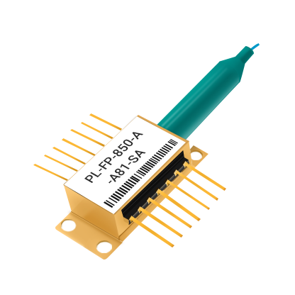


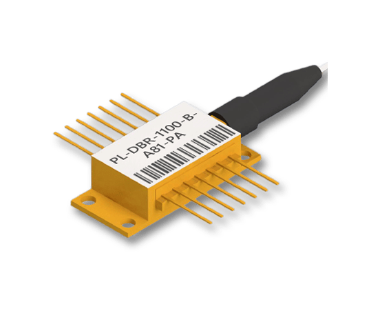


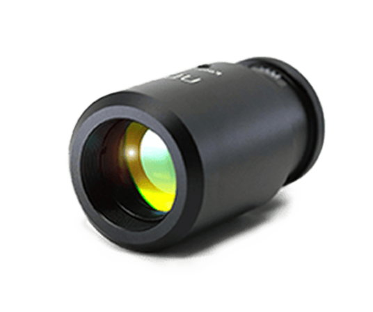


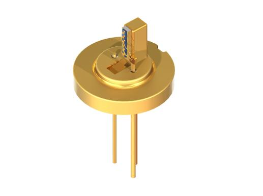
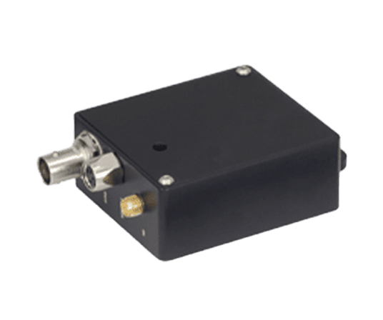
1060nm 210mW TypeB Gain Chip (TO Package)
A B-type (curved stripe) gain chip with TO packaging, with a center wavelength of 1060nm, designed specifically for external cavity semiconductor lasers. The chip is coated with a deep anti reflection (AR) coating on both end faces and relies on external frequency selective elements (such as diffraction gratings) to generate laser, thereby achieving a wide tuning range and high edge mode suppression ratio.
Product features:TO package; high gain efficiency; wide tuning range; low noise; easy integration
Part Number:MP-GC-1060-150-210-To-B
Application area:Optical fiber communication | LiDAR | Medical equipment | Sensing system | Industrial processing
Add to Cart Request for Quotation Consult Favorite
Center wavelength Tuning range Output power Forward current
1060nm 150nm 210mW 400mA
Recommended Operating Conditions
Parameter | Min. | Typ. | Max. | Unit |
Heat Sink Temperature | 20 | 25 | 30 | °C |
Forward Current* | — | — | 400 | mA |
Optical Feedback** | — | 20 | — | % |
* No self-lasing occurs at maximum current.** Excludes chip coupling efficiency.
Tuning Characteristics
Batch qualified under CW, 25 °C, 800 mA, external cavity with Littman configuration and 20% optical feedback.
Parameter | Min. | Typ. | Max. | Unit |
Maximum Power Wavelength | 1075 | 1090 | 1105 | nm |
Output Power @ 780 nm | 150 | 210 | — | mW |
Center Wavelength of Tuning Range | 1045 | 1060 | 1075 | nm |
Full Tuning Range Width | — | 150 | — | nm |
Side Mode Suppression Ratio (SMSR) @ 780 nm | — | 55 | — | dB |
Amplified Spontaneous Emission (ASE) Characteristics
Each device tested under CW, 25 °C, 800 mA, no optical feedback.
Parameter | Min. | Typ. | Max. | Unit |
Output Power | — | 20 | — | mW |
Forward Voltage | — | 2 | 2.3 | V |
Average Wavelength | — | 1015 | — | nm |
Bandwidth (FWHM)* | — | 35 | — | nm |
Fast-Axis Beam Divergence (FWHM) | 15 | 17 | 21 | deg |
Slow-Axis Beam Divergence (FWHM) | 5 | 8 | 11 | deg |
Polarization | — | TE | — | — |
* Radiative coupling into unlensed single-mode fiber, measured by OSA with 1 nm resolution.
Chip Parameters
Parameter | Min. | Typ. | Max. | Unit |
Chip Length | — | 1.5 | — | mm |
Front Facet Back Reflection | — | — | 0.1 | % |
Rear Facet Back Reflection | 90 | 99 | — | % |
Absolute Maximum Ratings
Parameter | Min. | Max. | Unit |
Forward Current @ 20% Feedback | — | 600 | mA |
Optical Feedback (Excluding Chip Coupling) | — | 30 | % |
Reverse Voltage | — | 1 | V |
Operating Temperature (Above Dew Point) | -10 | 60 | °C |
Storage Temperature (Original Sealed Package) | -40 | 85 | °C |

General Specifications
There are two types of external cavity lasers utilizing diffraction gratings: the Littrow configuration and the Littman/Metcalf configuration. In the Littrow structure, the first-order diffracted light from the grating is directly fed back into the semiconductor laser, and laser oscillation is realized through resonance with the low-reflection (LR) coated vertical facet. Since diffraction occurs only once, a higher optical output can be obtained compared with the Littman scheme.
Wavelength scanning is realized by rotating the diffraction grating. In general, an intra-cavity achromatic lens is adopted to collimate the expanded beam covering a large area on the grating. The zero-order diffracted beam serves as the output laser beam. The product line of Innvolume gain chips is divided into two main categories:
Single-sided optical access (Type A & Type B)
Double-sided optical access (Type C & Type D)
Single-fiber-access gain chips are ideal components for schemes where output power is coupled outwards from the external cavity. They are commonly packaged in transistor outline can housings. Dual-fiber-access gain chips are applicable in solutions that realize power output coupling from the gain chip facets to reduce optical loss, or in optical amplification systems.
Type A gain chips feature straight stripes perpendicular to the chip facets, with high-reflection and anti-reflection coatings. They provide a cost-effective solution for constructing external cavity diode lasers. Featuring symmetric far-field beam profiles, Type A chips achieve efficient coupling with external cavities and rear cavities when paired with high-numerical-aperture aspherical lenses. This type exhibits relatively limited gain spectrum ripple suppression, as the reflectivity of the anti-reflection coating is maintained at approximately 0.1%. The residual reflectivity can be further reduced via curved stripe-to-facet design optimization.
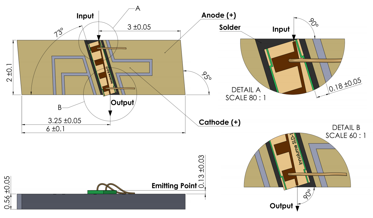
Type B gain chips are designed with curved stripes, adopting a high-reflection coating on the normal facet and a deep anti-reflection coating on the tilted facet. The combination of curved stripes and advanced anti-reflection coatings delivers ultra-low facet reflectivity (< 10E-5), effectively suppressing self-lasing and minimizing gain fluctuation. A drawback of curved stripes is output beam distortion, which complicates beam collimation and reduces reverse coupling efficiency. High-numerical-aperture optical elements are therefore mandatory for practical operation.
Type C gain chips incorporate curved stripes and anti-reflection coatings on the tilted facet, with a moderate reflectivity of several percent on the normal facet. Wavelength-selective optical feedback is configured on the tilted side, sharing the same merits and limitations as Type B, while optical power is extracted from the normal facet. This configuration enables high output power and superior beam quality. The reflectivity of straight-stripe facets needs customized optimization according to system configurations and target output power.
Type D gain chips adopt tilted stripes with anti-reflection coatings on both facets, primarily designed for advanced optical systems requiring integrated amplification units. Innovative facet coating technology combined with facet passivation ensures long-term operational reliability. Manufactured in compliance with ISO9001:2008 standards, all products undergo rigorous design, standardized fabrication and comprehensive testing. Each device is individually characterized and delivered with complete test data reports.


Characteristic Curves
Typical Performance in External Cavity (For Reference Only)
Optical Spectra(res. 0.5 nm)

Optical Spectra(res. 10 pm)

Output Power Spectra

Integrated Signal/ASE ratio

Output Power@1090 nm

Threshold Current

Typical Performance without feedback(for reference only)
L-I-V Curve

ASE Spectra(res. 1 nm)

Operating Instructions
Safety and Operating Instructions
The light emitted by this device is invisible and hazardous to human eyes. Avoid direct viewing of the fiber connector while the device is in operation. When operating with the connector uncovered, appropriate laser safety goggles must be worn.
Absolute maximum ratings shall only be applied to the device for a short duration. Long-term exposure to maximum ratings or simultaneous exposure to multiple maximum ratings may cause device damage or reliability degradation. Operation beyond the device’s maximum ratings may result in equipment failure and potential safety hazards. A dedicated matched power supply must be adopted to ensure the maximum forward current is not exceeded.
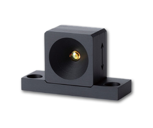
Devices mounted on heat spreaders require a qualified heat sink. The device shall be fixed to the heat sink with 4 screws (fastened in a cross pattern with an initial torque of 0.075 N·m and a final torque of 0.15 N·m) or clamps. The flatness deviation of the heat sink surface shall be less than 0.05 mm. Indium foil or flexible thermal interface materials are recommended between the device base and the heat sink. Thermal grease is not recommended for this application.
Prevent optical back-reflection, which may degrade the device’s spectral performance and output power stability, and even cause catastrophic facet damage. An optical isolator is strongly recommended to suppress back-reflection.
Do not pull the optical fiber. Avoid bending the fiber with a bending radius less than 3 cm. The fiber end-face shall be fully protected against contamination and mechanical damage during installation. After removing the dust cap, clean the fiber end-face unidirectionally with lens cleaning wipes or cotton swabs moistened with isopropyl alcohol or ethanol. Operate the device only with clean optical fiber connectors.
ESD Protection
Electrostatic discharge is a primary cause of unexpected product failure. Strict ESD precautions must be implemented at all times. Maintain continuous ESD protection during installation, including the use of anti-static wristbands, grounded work surfaces, and standardized anti-static operating procedures.

--
Request for Quotation
We will reply to all your information about the product in time.
⇪